Our Courses


70
Courses
34000
Members
12
topics
7
locations
Popular Courses
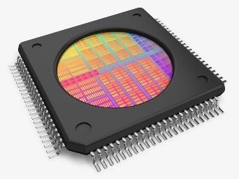
Dr. Jeffrey Gambino, ON Semiconductor, United States, is teaching this advanced 5-day course, which will provide an high-level overview of the entire fabrication process of modern Silicon-Based Integrated Circuits.
This course includes all the key materials involved and the process areas utilized in device manufacturing. The course is addressed to a broad audience and is not intended as a research review, although it will be taught at a high level and in many areas will require familiarity with the subject matter.
Professor Albert J.P Theuwissen, Delft University of Technology, the Netherlands and Harvest Imaging, Belgium is the instructor for this 3-days course in how to get familiar with Solid-State Imaging and relevant related topics.
If "A picture tells more than a thousand words", then imaging was and still is the language of the future. In today's emerging markets of electronic equipment, imaging plays a very important role. The art of imaging and image processing is working its way into the automotive scenes, wearables, IoT, AR/VR and taking on environmental challenges. Solid-state image sensors are present in diverse professional application areas.
The major objective of this course is to make the participants familiar with solid-state imaging and the relevant related topics. It will give an in-depth view of the possibilities and limitations of the Image Capturing Technology of today and tomorrow.
***
For best training experience, we recommend the adjoining 2-day course #020 Advanced Course on Image Sensor Technology, also taught by Professor Theuwissen.
If booking both these courses in the same week, the total course fee will be EUR 3540 pp (Early Bird) or EUR 3935 pp (Regular fee)
Dr. Farzad Parsaie, founder of SAND Microsystems GmbH, Switzerland is teaching this 2-day course in Optical Sensors.
Optical Sensors have got a broad range of applications from automotive sensing for autonomous driving (AD) and advanced driver assistance systems (ADAS) to many other areas such as industrial sensing and scanning, gas sensing, 3D Imaging. Optical sensors are also used in robots, drones, medicine, aerospace and for optical communication systems. Many test and measurement systems include optical sensors to get higher accuracy.
This course deals with optical sensors that need to be very sensitive and/or high-speed. It starts from the physics of optical detectors and properties of light to the interaction between photons with the semiconductor material. It handles important items like noise, sensitivity and switching speed by analyzing major factors determining them. In the second part different topologies for electronic interfacing and signal conditioning to the Analog/Time to Digital Conversion (ADC/TDC) will be introduced and covered. Challenges and suitable Technologies for integration in Application Specific Integrated Circuits (ASIC) will be introduced to reduce size and cost.
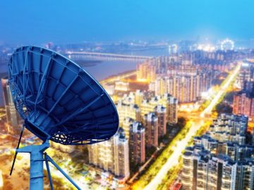
Mr. Geoff Varrall, Executive Director of RTT Programmes, UK, is teaching this 5-day course.
This course provides a comprehensive introduction to the system and service aspects of low and high-count LEO, MEO and GSO satellite constellations but also studies the integration of 5G and 6G networks (non-terrestrial network integration including sub orbital and aerospace) and RF and optical integration.
In 2018, the average payload for a rocket was of the order of 5 metric tons. By 2023 that had increased to more than fifty tons (typically 100 to 150 tons) with visibility of payloads per launch scaling to 500 tons on top of a 5000 metric ton rocket. The construction of the International Space Station (450 tons) required 50 journeys into space. We now have visibility to launching a platform of similar size and weight on a single rocket.
This is transforming the economics of delivering RF and optical hardware into LEO, MEO and GSO orbit, in particular, enabling the LEO market to scale from 500 to 5000 satellites with the potential to increase to 50,000 or more over the next five years. LEO satellites are getting bigger (2000 rather than 200 kilogrammes) which means that they can support multiple payloads including RF and optical communications, RGB and multi/ hyper spectral imaging, RF trilateration and Synthetic Aperture Radar. The satellites by default collect large amounts of data directly useful to space science and research.
The technology economics of satellite are therefore undergoing profound transformation. In parallel telecommunication engineers and regulators need to understand the interference and competition policy dynamics of these new multi orbit constellations and to be up to date on how optical cross links and optical space to ground and ground to space links are changing the architecture, functionality and performance of space and terrestrial networks and potentially resolving emerging space based and space to earth and earth to space RF interference issues. If you are interested in any of the above, this course is for you.

Dr. Sorin Fericean is the instructor for this 5-day course on how to get familiar and experienced with the extremely large types and versions of sensors for industrial applications.
He is a new instructor of the CEI-Europe and is a professional expert on the subject of design and manufacturing of electronic sensors and ASIC designing, testing, and release for such products. After more than 25 years with one of the 10 global players on the field of industrial sensors – Balluff GmbH Company, Germany – he is currently as a freelancer in his consulting office FerSensC / Leonberg, Germany, carrying out sensor design projects and consulting.
Latest from our Blog
Recent Blog Posts
Due to the ongoing pandemic, majority of our courses are taught online this Autumn.
Here is an example from Dr. István Novak´s course in Power Integrity Distribution.
https://vimeo.com/575826305/98901439f7
Our course portfolio is for the public and also available to book as inhouse events.
Contact us for further details! cei@cei.se
World's premier conference for chip, board, and systems design engineers in the high-speed communications and semiconductor communities announces winner of prestigious award.
DesignCon, the nation’s largest event for chip, board, and systems design engineers, today announced Dr. István Novák, Principal Signal and Power Integrity Engineer, Samtec, as the 2020 winner of its prestigious Engineer of the Year Award. The Engineer of the Year Award recognizes the best of the best in engineering and new product advancements at the chip, board, or system level. Each year, the award winner receives a $1,000 grant or scholarship to present to the educational institution of their choice. Dr. Novák has selected to do
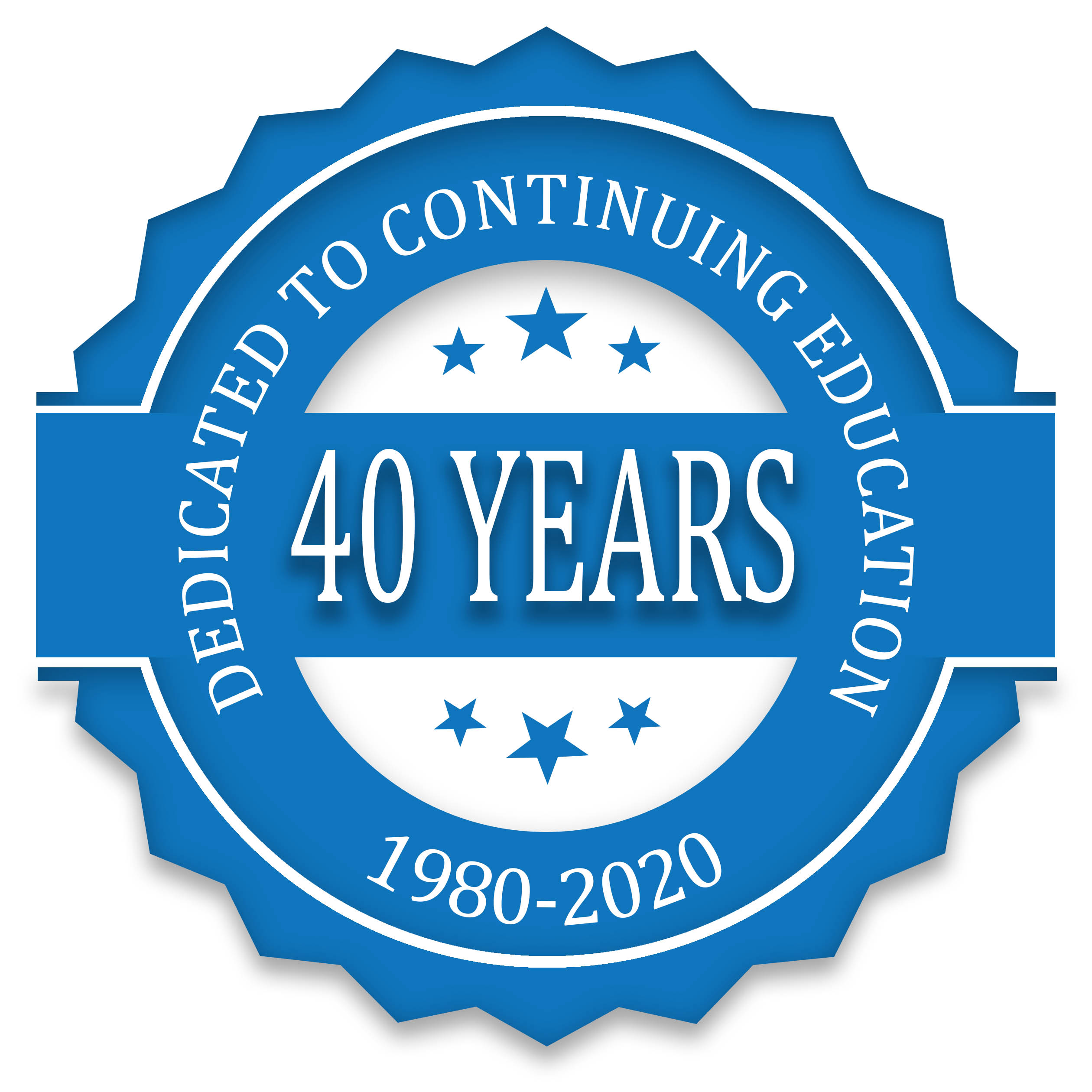
Dedicated to Continuing Education since 1980, we are happy to announce our 40th anniversary as technical training provider!
Our vision and objective has always been to offer an arena to European professional engineers where technical know-how is transferred. By offering high-quality training, companies will attract and keep their talents.
We are very happy and eager to continue our journey in the educational field. Providing spearhead technical education makes a difference between yesterday and tomorrow for our customers and we like to be at the forefront every step of the way.
This is what we know and care about!
Deepest Thank You to our instructors, from the past and present, for dedicating their time and passion to teach, give guidance and support to our customers and our office. Without you, this would not have been possible!
A huge Thank You to the returning engineers, keep coming back for the latest updates in your technical field -
We are happy to announce that we have signed an agreement with the company Astute in Bangalore, India.
Astute (meaning Trust, Future) is a Technology Solution provider in the areas of Blockchain, IoT, Robotics, Virtual Reality / Augmented Reality, Artificial Intelligence, Robotics, 3D printing and Smart City Solutions.
We are looking forward to a fruitful collaboration with successful marketing of our technical courses to engineers across India.
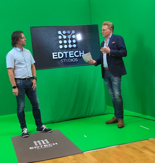
E-Learning being on all lips when talking about Continuing Education. We are happy to annouced new partnership with the experienced e-Learning production team of EdTech Studios in Torsås, Sweden.
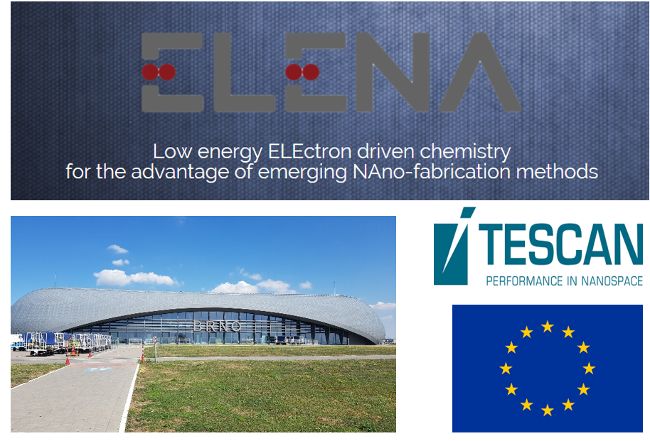
Excellent collaboration with Tescan ME for the 2nd Technical Training School within the ELENA project. 15 PhD students from Iceland, Czech Republic, Germany, Norway, Switzerland, Belgium, Austria, UK and,The Netherlands, together with supervisors also from USA, France and Poland, are funded from the EU Horizon 2020 Research and Innovation programme under the Marie Sklodowska-Curie Action. FEBID, precursors, electrons, Electron and Ion Beam Nanolithography are discussed together with SEM Detection Systems.
Digital Marketing Officer
We are looking for you who wants to develop and streamline our company's digital marketing. You will, together with the CEO / Marketing Manager, put up campaigns in different digital channels, as well as follow up and analyze them.
We would like to see you having a postgraduate degree, preferably with focus on Digital Marketing or a few years of experience with similar tasks. You need to have knowledge of digital marketing, campaign work and follow-up and analysis of data. Since our market is international, you need to master English fluently in speech and writing. It is an advantage if you can have additional language skills.
We believe that you have previously published some texts, articles or blogs and can easily communicate in both spoken and written terms. You think digital marketing is an exciting area and wish to learn more about how to market an online business. You are also analytical, result-driven

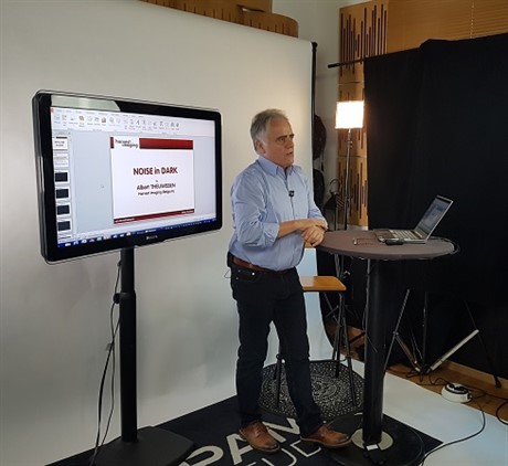
The long-term partnership between CEI-Europe and Professor Albert Theuwissen continues with the release of a three-part eLearning course on Correlated and Uncorrelated Noise in Imagers.
Since the late nineties, CEI-Europe and Professor Albert J.P. Theuwissen have delivered courses for engineers, expanding knowledge in the areas of Digital Imaging, Image Sensors Technology, and Digital Camera Systems. Now, the longtime partners take another step by presenting courses in the eLearning format, making the access to obtain Dr. Theuwissen’s expertise readily available for a global audience.
The three-part course begins with the section ”Introduction to Correlated and Uncorrelated Noise in Imagers”, wherein the difference between Correlated and Uncorrelated Noise is explained. The second part, ”Characterization of Noise in Dark”, covers the performance of Image Sensors in Dark. Th
Exiting news!
Our first E-learning course is now in production! See the introduction film on youtube!
We have chosen the very popular course in 004 Hands-on Characterization of Solid-State Image Sensors, taught by Professor Albert Theuwissen. He is now in action at Pama Studios, Kristianopel/Sweden.
We plan to go public with the course by March 2018 - more info will follow.
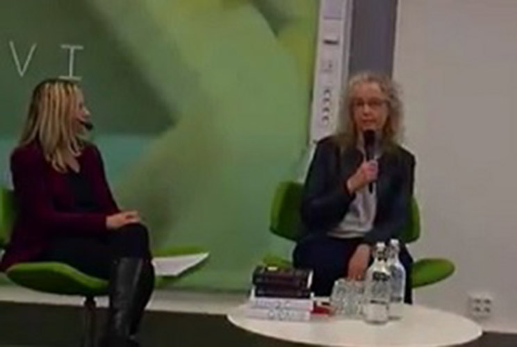
Our CEO Ann-Charlotte Johannesson was interviewed at Mjärdevi Science Park on Friday the 19th.
The discussion is on Continuing Education, something we are of course familiar with! The importance of education and our role in having educated over 33 000 persons so far, and how we are implementing e-learning to reach even further.
Subscribe for a newsletter
Select the technical category of your interest! By signing up to our Newsletter, you will allow us to send you relevant course information. In compliance with GDPR, your email address will not be used in any other way.