
TECHNOLOGY FOCUS
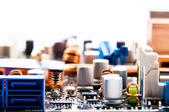
The rapid growth of the semiconductor industry has relied on the continual evolution of materials and processing compatible with fabricating modern silicon-based integrated circuits. Continuous feature scaling has led to increased integration, lower cost, higher speed, and compactness, however, the challenges of fabricating smaller feature sizes has demanded advances in materials processing. More recent demands include lower energy consumption and expanded functionality. Advances include strain engineering with Ge alloying, Silicon-on-Insulator (SOI), penetration of Cu metallization and required barrier materials, and development of high κ dielectrics.
COURSE CONTENT
This course will provide an overview of the entire fabrication process. It will include all the key materials involved and the process areas utilized in device manufacturing. This course is thus addressed to a broad audience and is not intended as a research review, although it will be taught at a high level and in many areas will require familiarity with the subject matter.
WHO SHOULD ATTEND
Monday
Si Front-end Manufacturing
An overview of the entire front-end manufacturing process will be presented. A perspective on process bottlenecks and future trends is presented.
- Si Wafer Production
- Epitaxy
- Oxidation
- Dielectric Deposition
- Ion Implantation
- Metallization
- Lithography
- Etching
Device Technologies and Semiconductor Materials
The basic device technologies will be discussed, including bipolar and CMOS.
- Electrical, Optical, and Structural Properties of Silicon
- Control of the Point and Extended Defect Densities
- Origin of Defects and Their Influence on Device Performance
- IC Materials Characterization for Process Improvement and Achieving High Yield
Process Induced Defects and Device Performance
Common impurities introduced during materials growth and their influence will be discussed. The crystallography of the diamond structures and the formation mechanisms and structures of extended defects, i.e. stacking faults, misfit dislocations, twins, will be reviewed. Both intrinsic and extrinsic gettering technologies will be described with a discussion of their effects on subsequent device processing and device parameters.
Silicon Epitaxy by CVD
Silicon epitaxial deposition is a strategic process technology in large volume manufacturing. The understanding and control of this technology is critical to the success of the production of high quality devices and circuits. Topics to be covered include:
- Substrate Crystal Orientation, Deposition Parameters, and Choice of Silicon Source Material
- CVD Fundamentals for Si Deposition Chemistries
- The Influence of Deposition Parameters on Film Quality
- Procedures to Prepare Wafers for Epitaxy
- Film Quality and Device Performance
- Si Etching by Wet Processes
- Isotropic and Anisotropic Etchants
Emerging Substrate Technologies
Several technologies are emerging to meet the demands for higher speed, higher density, and lower voltage integrated circuits, as well as a broader range of applications including IoT, rf and power electronics, and biomedical devices. Growth of SiC or GaN on Si is now found in power and rf devices, while Silicon-on-Insulator (SOI) technology is now commercially available. Furthermore, the SixGe1-x alloy is another advanced material that was recently introduced into the marketplace. The impact of the growth process on the properties and an overview of the device applications will be presented.
Tuesday
Silicon Oxidation
The role of the native oxide of Si as an enabler of advanced Si technology cannot be overstated. This section outlines the fundamental aspects of silicon oxidation.
- Gate Oxide, Surface Passivation, Mask, Device Isolation
- Growth Models for Wet and Dry Oxidation
- Surface Preparation
- Charge and Atom Transport
- Dopant Redistribution
- Orientation Effects
- Properties of Ultra-thin Oxides
- Novel Processes such as Rapid Thermal Oxidation
Deposition of Metals and Dielectrics by Physical and Chemical Methods
The various physical and chemical approaches to the deposition of metal and dielectric materials are outlined and compared. The 'Roadmap' predicts that Atomic Layer Deposition (ALD) methods will eventually become the dominant process because it is well suited for deposition of ultra-thin, highly conformal films over small device features.
CMP for Microelectronics Applications
Chemical Mechanical Planarization (CMP) is an enabling technology for the microelectronics industry. The empirical nature of CMP and how it bridges many engineering disciplines for resolution of its numerous challenges will
be emphasized.
- How to Effectively Utilize CMP
- Evolution and Revolution of CMP Equipment and Consumables
- Characterization Techniques for Process Development and Control
- Advantages and Limitations of CMP Processes for
- Advanced Microelectronics Applications
High k Dielectric Materials
Alternate gate dielectric materials are being developed, as the continuously reduced SiO2 thickness is approaching its physical limitation and direct electron tunnelling results in unacceptably high leakage currents.
- Potential High k Materials
- The Impact of Thin Gate Oxides on Device Performance
- Benefits of the Use of High k Dielectrics
- Material Properties, Growth Methods, and Impact on Device Performance
Wednesday
Optical Lithography
The continuous trend of miniaturization in IC manufacturing and the importance of lithography as an enabling technology will be presented.
Optical lithography has till now always been the workhorse of the industry. The lithographic process of optical lithography will be analysed.
- Image Formation in the Optical Lithography Process
- Basics of the Resist Chemistry
- Issues Encountered when Applying Resists to Real Device Processing
- Resolution Enhancement Techniques: Phase shifting masks, off-axis illumination, optical proximity correction
Recently, 193nm immersion lithography, double patterning and 13.5nm EUV lithography have been introduced techniques for further scaling the resolution limits of optical lithography. This section will address the current status of each technology and the technological challenges for each of these new technologies and discuss the anticipated insertion points.
Plasma Etching and Plasma-Enhanced CVD
- This section covers the fundamentals of plasma processing, including plasma-enhanced chemical vapor deposition and reactive ion etching (RIE).
- Reactive Gas Glow Discharges: Plasma etching, reactive ion etching, and PECVD
- Operation of Low and High Density Plasma Sources
- Surface Science Aspects of Plasma Etching
- The Role of Energetic Ion Bombardment in Obtaining Etch Profile Anisotropy
- Etching of Silicon and Its Compounds in Halogen-based Etching
- PECVD and Its Role in Plasma Etching
- PECVD Processes of Greatest Importance in Semiconductor Manufacturing
Ion Implantation and Diffusion
Critical issues of ion implantation and junction formation in silicon devices are discussed.
- Device design; CMOS, Bipolar, Power, Sensors,
- Process Issues in Applying Ion Implantation/Annealing
- Materials Issues of Ion Penetration, Damage Production, and Masking
- Annealing Implanted Layers in Silicon: Oxidation over implanted layers, furnace annealing, Rapid Thermal Processing (RTP)
- Critical Issues for Creating pn Junctions in Silicon: Low leakage junctions, removing damage, controlling diffusion during the annealing of implantation damage, scaling of pn junction depths, contacting, diffusion through thin oxides in doped polysilicon gate/oxide/ silicon devices
- Process Simulation for Design and Control of Implanted and Annealed Junctions
Thursday
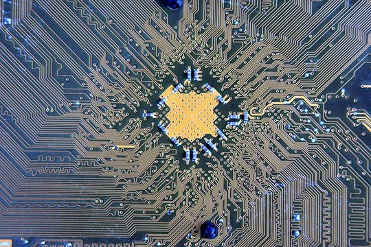
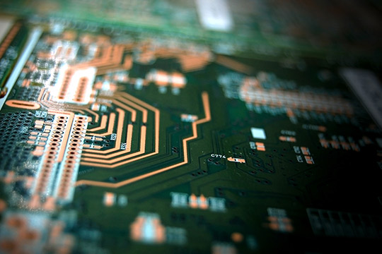
Integrated Circuit Metallization Systems
- The scaling of VLSI and ULSI circuits and the impact on the performance and density of interconnects will be reviewed. Current interconnects with Cu and low k dielectrics and recent development on 3D interconnects will be discussed. Multi-layered Interconnect Structures: High density and high performance
- Scaling and Wiring Requirements of ULSI Circuits
- Interconnect Performance and Density
- Requirements for Metallization Systems in Device Contacts and Interconnecting Lines
- Aluminum BEOL with SiO2 dielectrics
- Copper BEOL with Low k Dielectrics
- Basic packaging processes
- Recent development on 3D interconnects
Friday
Reliability and Yield
The success of an IC manufacturing facility is directly connected to IC reliability and product yield. An overview of failure mechanisms and yield limitations will be presented. The discussion will include approaches to circuit and layout design, device design, materials selection, process optimization, as well as thermo-mechanical considerations. Proven yield improvement management processes will be outlined.
Said about the course from previous participants:
" Information about advanced manufacturing technology."
" Video to illustrate fab work. Future process and future technology."
" Good view on new technologies - latest developments."
" The talent and strong background of the lecturers."
"Widely covered aspects, get a feeling how each discipline is working and thinking."