
TECHNOLOGY FOCUS
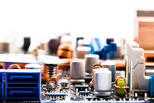
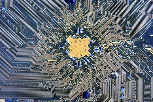
Microelectronic products and systems are essential to modern society. They appear in lightweight, low-power consumer applications such as mobile communication, as well as in high-power industrial applications like automotive electronics and aerospace systems. At the heart of every microelectronic system is the integrated circuit (IC), fabricated using planar processing technology. In this fabrication process, patterning of planar surfaces plays a crucial role. The demand for greater functionality at lower costs has driven an increase in patterning density—a trend known as Moore’s Law. Optical lithography has remained the primary patterning technology, enabling the minimum feature size to shrink from 10 µm in 1970 to just 5 nm in modern production. Although novel optical lithographic tools and technologies have emerged, they continue to rely on the same fundamental principles. Furthermore, new trends in micro-system fabrication, 3D integration, and advanced packaging require innovative applications of these foundational lithographic techniques.
COURSE CONTENT
This course explores the fundamental lithographic principles and technologies, explained through both theoretical concepts and practical experiments. Since lithography is integral to IC fabrication, the course emphasizes lithographic techniques within key IC process technologies. A full basic CMOS process flow is examined, highlighting lithography's impact on device performance. Additionally, lithography applications in micro-system technology and advanced packaging are reviewed.
The course structure includes 60% theory and 40% practice, ensuring hands-on experience supports the theoretical foundations.
Practical experiments take place in a class 100 cleanroom, equipped for the fabrication of CMOS circuits. These experiments are scheduled throughout the week, closely aligned with theoretical sessions to enhance learning.
WHO SHOULD ATTEND
This course is designed for engineers, researchers, and students from both industry and academia who are engaged in IC fabrication, microsystem technology, or advanced packaging—whether in research, product development, or hands-on applications. Participants will gain a detailed understanding of lithographic principles and technologies, providing them with essential expertise for both professional and academic applications.
General Physics and Chemistry prior knowledge is needed to follow the course.
____________________________ DAY 1 ____________________________
- Introduction
History and trends in the IC industry and the evolution of lithographic exposure tools.
An introduction of semiconductor device fabrication principles
- Device process examples
The main IC fabrication technologies are discussed together with the effect of variations in the main lithographic parameters like line width and overlay on the IC device performance
____________________________ DAY 2 ____________________________
- Cleanroom technology
A brief overview of the main cleanroom parameters is given. The impact of cleanroom conditions on the lithographic processes and yield is discussed.
- Inspection and linewidth measurements
Practical inspection and linewidth measurement technologies are given in this chapter
- Optical imaging
The basic theory of optical imaging; the resolution limit, depth of focus are discussed together with advanced optical imaging and resolution enhanced technologies.
____________________________ DAY 3 ____________________________
- Thin film optics
The interference effect in thin films and the consequence on optical imaging is explained. The swing-curve and the application of anti reflective coatings is explained as well. Experiments are used to support the theory
- Photoresist chemistry and processing
The operating principle of I-line photoresist is explained in theory and with experiments. DUV resist technology is dealt with as well and alternative resist processes like image reversal and thick resist processing will be discussed briefly
____________________________ DAY 4 ____________________________
- IC technology, micro system technology, packaging and lithography
A complete CMOS process flow is reviewed in relation with lithography. For each IC process step the consequences of the lithographic process flow will be explained.
____________________________ DAY 5 ____________________________
- Micro system technology, packaging and lithography and lithography
The specific challenges for lithography in the field of micro system technology and packaging will be reviewed
- Process engineering and process control
A lithography process is a multi parameter process. The knowledge of the previous chapters will be applied to identify the critical parameters in a lithographic process and to set up a lithographic process for different applications
- Questions & Answers