
TECHNOLOGY FOCUS
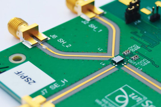
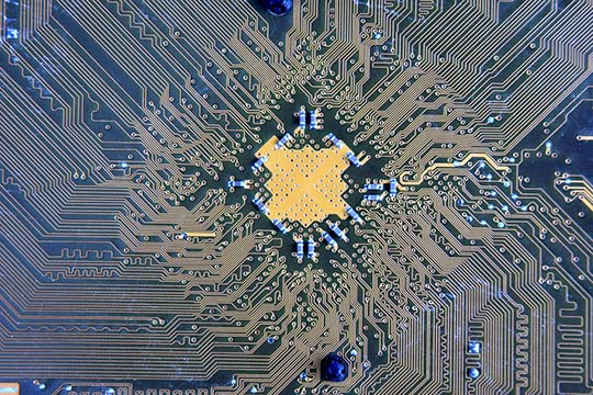
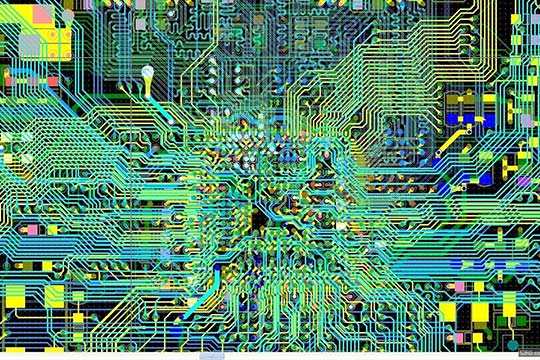
All EMI problems begin and end on the Printed Circuit Board. In recent years, PCBs have become increasingly complex. The use of high density VLSI on the one hand, combined with the increased processing speed and data rates on the other hand, have led to the increased density of the circuits. The use of high speed/high edge rate digital circuits, along with the need for low power consumption, have contributed to higher electromagnetic emissions from circuits, on the one hand, and increased sensitivity of the circuits on the other, leading to Electromagnetic Interference (EMI) problems.
A special problem is that of Signal Integrity (SI). For the adequate control of EMI, strict international standards and regulations have been developed worldwide. These standards require the suppression of electromagnetic emissions from circuits and systems, and their increased immunity to externally induced interference. The proper design of PCBs is a cost effective approach for the control of EMI in high-speed circuits.
COURSE CONTENT
This is an advanced design course, dealing with the theory and design of PCBs for meeting EMC and SI objectives.
The course features understanding of the electromagnetic phenomena in PCBs, and in particular in high-speed digital PCBs.
The course emphasizes practical applications, with mathematical derivations kept to the minimum necessary.
In addition, case studies and practical "real life" examples will be provided.
WHO SHOULD ATTEND
Day 1
Introduction - Why Design for EMC and SI?
We will discuss the concepts of EMC and SI and describe the similarities and differences between the two as they pertain to circuit design and the primary parameters that govern interference modes and system performance with respect to EMC and SI.
Noise Sources on PCBs
The characteristics of noise sources on PCBs will be discussed, with particular emphasis on noise in signal, power and ground circuits. Coupling and interaction between circuits, particularly crosstalk, will be discussed in detail.
Circuit Elements
Characteristics of real world circuit elements, with special emphasis on parasitic inductance, capacitance and resistance will be discussed.
Fundamentals of Grounding Design
The concept of grounding and basics of grounding system designs will be presented. Design of the grounding tree and identification and elimination of ground loops will be discussed in detail. Application of the fundamental grounding theory to grounding on PCBs will be presented.
Day 2
Power Circuit Designs on PCBs
A discussion of the interaction via the power system on the PCB will lead to the concept of decoupling, classical and innovative decoupling strategies, filtering, and filter design for EMI control. In particular, the generation of Parallel Plate Waveguide Noise will be discussed. Novel techniques for addressing "Ground Bounce" or delta-I Noise and its mitigation such as Electromagnetic Band Gap (EBG) will also be presented.
Reflections and Impedance Mismatch on High Speed Digital PCBs
We now focus on the treatment of signal traces, transmission lines, and the implication of the concept to PCB design. Impedance mismatch, leading to reflections and noise are discussed in detail, and design approaches, including impedance matching, source and load termination topologies are presented. The concept of "S-Parameters" for circuit analysis will be presented.
Day 3
Crosstalk on the PCB
The concept of crosstalk on PCB as a primary source of EMI concerns and failures is discussed. Approaches for minimizing crosstalk, with particular emphasis of routing guidelines, are presented in detail.
PCB Design for EMC
Strategies for a systematic design approach of PCBs from the standpoint of EMC and SI includes such design features as layout, layer stacking, placement, power distribution and grounding/reference systems.
Treatment of Mixed (Analog/Digital) Circuits
The problem of mixed analog/digital circuits is presented. The discussion covers the problem of ADC and DAC devices, and circuit design with one or multiple devices on one and on multiple PCBs.
Day 4
Clock Circuits
The special problems associated with clock circuits and clock signal distribution, including classical and novel approaches for clock circuit design, are discussed.
Treatment of Special Signals in PCB Design
Some commonly used digital interfaces, such as LVDS circuit design, are given particular attention.
Shielding on PCBs
Implementation of shielding as an EMI control measure, particularly on PCBs, is discussed here.
Edge Connectors
Improper design of edge connectors may cause an otherwise good design to fail both EMC and SI objectives. We will discuss the proper design of edge connectors consistent with circuit design with special emphasis on high-speed interfaces. Items covered include pin allocation, layout of power, ground pins, and the connector arrangement.
PCB Layout Guidelines
A verification checklist for PCB layout guidelines for EMC and SI will be presented.
Day 5
Measurement Fundamentals
EMC measurements, particularly the use of spectrum analysers and oscilloscopes for observing system performance, will be discussed.
Summary
Questions, examples presented by the participants, and practical EMC and SI problems on PCBs will be treated in an interactive manner.
Said about the course from previous course participants:
"The course was relevant to all important aspects of PCB design."
"I liked both the SI and EMI teaching as both are not always covered in the same course."
" Right balance between theory and practical point of view."
"Practical and real examples."
"The enthusiasm of the teacher makes the subject easier to learn."
"I like the concept of giving the basic understanding in the first days and then putting it all together in the end."