
TECHNOLOGY FOCUS
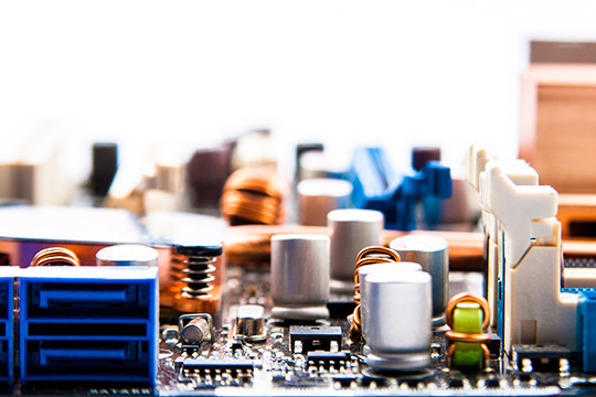
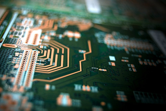
Microelectronic products and systems are essential to modern society. They are found in lightweight, low-power consumer applications such as mobile communication, as well as in high-power industrial applications like automotive electronics and aerospace systems. At the heart of every microelectronic system is the integrated circuit (IC), fabricated using planar processing technology.
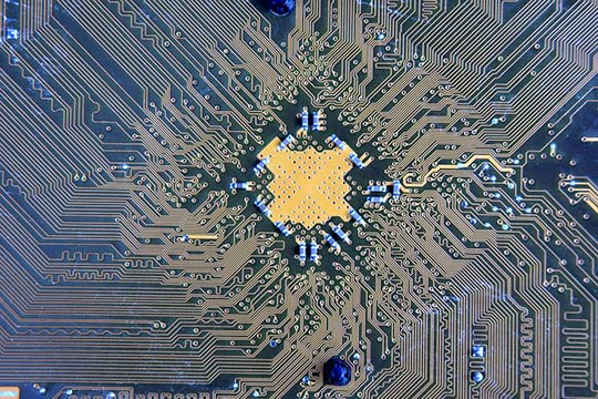
Since the invention of the integrated circuit in 1958, the microelectronics ecosystem—comprising intellectual property, materials, processes, and equipment—has developed tremendously. The core of this ecosystem is wafer fabrication, where fundamental technologies such as semiconductor doping, photolithography, etching, and thin film deposition have been key for decades.
The advanced microfabrication techniques developed for CMOS are now also being applied for other purposes, such as the manufacturing of micromechanical devices often combined with microelectronics (MEMS), or for advanced microelectronic packaging.
This course will discuss the basic principles and the interconnection of these core technologies as applied in a CMOS manufacturing process and in the fabrication of MEMS devices.
COURSE CONTENT
This course is an introduction to the fabrication technologies used for integrated circuits (ICs) and microelectromechanical systems (MEMS), also referred to as microsystems. The aim of this course is not only to bridge the gap between the physical world (the physics of the device) and the electronic world (the characteristics of the device), but also to demonstrate the intertwined relationship between the various process technologies applied in a sequence to manufacture devices and circuits. In this way, participants will gain a better understanding of the critical aspects and challenges of integrated circuit manufacturing.
The course begins with a discussion of basic microelectronic devices, including a brief review of the underlying physics. The associated basic fabrication technologies required to create these devices are also covered. Next, mainstream IC fabrication process technologies are discussed in more detail in dedicated chapters, including their physical motivations and impacts on device characteristics.
In a separate section, typical fabrication technologies for MEMS devices, such as silicon bulk and surface micromachining, are presented to illustrate the potential of 3D micro-structuring in the development of microsystems or MEMS. These IC-compatible technologies are used to build multifunctional systems for a wide range of scientific and industrial applications.
Finally, a typical CMOS process flow is discussed in detail, with an emphasis on how the various process techniques are integrated into the fabrication sequence.
WHO SHOULD ATTEND
This course is designed for engineers, researchers, and students from both industry and academia who are engaged in IC fabrication and microsystem technology, whether in research, product development, or management. Participants will gain an overview of the basic manufacturing technologies and their intertwined applications in a CMOS process flow. This course will provide an essential background for further specialization in more specific process technologies or interdisciplinary management, applicable to both professional and academic settings.
General Physics and Chemistry prior knowledge is needed to follow the course.
1. Introduction
This chapter provides a foundational introduction to semiconductor physics, tailored for those outside the field. It explores the different types of semiconductor devices, offering a broad overview of their functions and applications. Additionally, it examines the history and evolving trends in microelectronics, highlighting the continuous drive for further scaling. Finally, the chapter introduces the basic principles of microsystems and MEMS, outlining their significance in modern technology.
2. Silicon
This chapter explores silicon as the material of choice for semiconductor and MEMS fabrication. It covers the general properties of silicon, including its crystal structure and key physical characteristics. The electronic structure of silicon and charge carrier transport mechanisms are examined in brief to provide a basic understanding of its behaviour in electronic devices. Additionally, the chapter introduces the pn junction, discussing the depletion layer and current-voltage characteristics, which are fundamental to semiconductor device operation. The chapter concludes with an overview of silicon wafer fabrication, detailing the processes involved in producing high-purity wafers essential for modern semiconductor manufacturing.
3. From physic to devices
This chapter bridges fundamental semiconductor physics with the fabrication process flows of various semiconductor devices, ranging from a basic semiconductor resistor to a complementary metal-oxide-semiconductor (CMOS) process. For each device — resistor, diode, capacitor, bipolar transistor, and MOS transistor r— the key process steps are examined in relation to their electrical characteristics and performance. Additionally, the chapter explores the monolithic integration of these devices, discussing its advantages, limitations, and challenges such as cross-talk and design constraints.
4. Patterning and pattern transfer
This chapter is divided into two parts: lithographic patterning and the transfer of lithographic patterns into structured layers. In the first part, the necessity of patterning at micro and sub-micro scales is explained, along with the advantages of optical lithography and its pivotal role in microelectronics fabrication. The mask-making process is discussed, followed by the basic principles of mask aligners, wafer steppers, and wafer scanners. The basics of photoresist chemistry and processing are covered, leading to an overview of the exposure and development stages in lithographic patterning. In the second part, the principles of wet chemical etching are discussed, followed by a basic explanation of reactive ion etching. The chapter concludes with a brief description of additive manufacturing techniques such as lift-off, electroplating, and ion implantation.
5. Thin Film Growth and Deposition
The chapter on thin film growth and deposition covers various techniques commonly used in the fabrication of integrated circuits (IC) and microelectromechanical systems (MEMS). It begins with a discussion on the thermal oxidation of silicon, followed by an exploration of chemical vapor deposition methods, including epitaxy, low-pressure chemical vapor deposition, and plasma-enhanced chemical vapor deposition. Next, the principles of atomic layer deposition are examined. For each of these techniques, typical applications in IC and MEMS processes are provided. The chapter concludes with an overview of the principles of physical vapor deposition and its application in a basic interconnect process flow.
6. Doping and Junction formation
This chapter introduces the principles of dopant diffusion in silicon. It begins with a discussion on the basics of solid-state diffusion, followed by an explanation of the two main diffusion models used in semiconductor doping. The application of diffusion furnaces is briefly covered. Next, the principles of ion implantation and annealing are discussed, including thermal annealing and rapid thermal processing.
7. MEMS
In the MEMS chapter, silicon bulk and surface micromachining technologies are presented to illustrate the potential of 3D micro-structuring in the development of microsystems or MEMS. These IC-compatible technologies are used to build multifunctional systems in a wide range of scientific and industrial applications. The chapter begins with an overview of silicon bulk micromachining, detailing the processes involved in creating deep structures within silicon substrates. This is followed by a discussion on surface micromachining, which focuses on the deposition and patterning of thin films on silicon surfaces to create intricate microstructures.
8. Integration
In the integration chapter, we use a basic CMOS inverter circuit to illustrate the use of junction isolation and surface isolation with the appropriate bias conditions for reliable circuit operation. A bipolar NPN transistor is added to this process to demonstrate the combined process and layout options for integrating different types of devices. The limitations of the current process and the effects of parasitic devices and latch-up are also discussed.
Next, a 180 nm CMOS process is reviewed in detail to explain the application of techniques such as chemical mechanical polishing (CMP), lithographic overlay and critical dimension (CD) control, silicides, and copper metallization. The topic of integrated circuit yield is briefly discussed as well. The chapter concludes with a brief discussion of advanced gate structures for nanometer-sized transistors.