
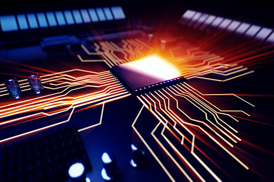
TECHNOLOGY FOCUS
With the continuous scaling down of semiconductor devices, interconnect technology and advanced packaging become increasingly challenging for product performance and reliability. For on-chip interconnects, fundamental changes in interconnect materials are needed with Cu replacing Al and low permittivity dielectrics replacing SiO2. The manufacturing of Cu/low-k interconnect stacks requires several single processes, including dual damascene patterning, Cu electroplating and chemical-mechanical polishing, as well as deposition of ultra-thin barriers and passivation layers. New materials and processes as well as their integration have to be understood to achieve high manufacturing yield and to mitigate product reliability issues. Reliability-limiting processes such as electromigration, stress-induced voiding in interconnects and time-dependent dielectric breakdown in ultra low-k dielectrics are reliability concerns.
Advanced packaging solutions, particularly 3D integration technologies such as wafer-level chip-scale packaging (WLCSP) and 2.5D/3D TSV integration, are an additional booster for performance and functionality of microelectronic products. However, at the same time, these approaches for 3D heterogeneous system integration are challenging for product reliability. Consequently, the role of reliability engineering increases particularly for target applications of 3D-stacked microelectronic products that have to be operated at harsh environments (temperature cycles, vibrations, etc.) with extremely high reliability. The manufacturing of 3D interconnect stacks is characterized by a broad variety of integration schemes and process flows, including processes such as silicon etch and metal fill as well as wafer thinning and wafer bonding. The 3D TSV integration process provides new challenges for processes (wafer thinning, TSV etch and fill), materials (materials compatibility, microstructure) and reliability (particularly stress-induced effects such as chip-package interaction). The role of multi-scale modelling and simulation as well as the need of accurate multi-scale materials parameters will be addressed in particular. Technological trends and specific applications, e.g. automotive electronics, will be discussed.
COURSE CONTENT
This course will provide an overview of processing, materials, performance and reliability aspects of on-chip interconnects and interconnects in 3D stacked integrated circuits. It will focus on basic issues related to integration schemes and process flows for damascene structuring of Cu/low-k stacks, WLCSP as well as for 2.5D and 3D TSV integration with and without interposer. Materials-related challenges, reliability issues and emerging applications will be discussed.
The course will include interconnect systems development for specific applications such as highly reliable automotive electronics. Technology trends of interconnect design and advanced packaging concepts of future microelectronic products will be discussed
WHO SHOULD ATTEND
This course is intended for engineers who wish to expand their knowledge in on-chip interconnects and advanced packaging, including concept, technology, materials, performance and reliability aspects of 3D interconnect systems of microelectronic products.
On-chip interconnect technology and advanced packaging
Trends in interconnect technology and concepts for advanced packaging
The ongoing trend of IC down-scaling of CMOS devices and it’s impact on interconnect performance and reliability will be reviewed. On-chip interconnects stacks with copper interconnects and low dielectric permittivity (low-k) materials as well as advanced packaging including 3D integration of chips will be introduced. As a consequence of the down-scaling of CMOS devices, the gap between to the slower down-scaled dimensions of printed circuit boards (PCBs) has been increased during the previous decades. Advanced packaging solutions, particularly 3D integration technologies, have the potential to bridge this gap between traditional Si ICs and PCBs. 3D heterogeneous system integration will be an additional booster for performance and functionality of microelectronic products. Past and future advanced packaging technologies, including wafer-level chip-scale packaging (WLCSP) and 2.5D/3D TSV integration, will be discussed.
On-chip interconnects: Processes and materials, and their integration
Multilayered on-chip interconnect structures designed to achieve high density and high performance will be discussed. Al metallization technology will be compared with Cu metallization technology. Various thin film deposition processes such as evaporation, sputtering, chemical vapour deposition (CVD), plasma-enhanced CVD, atomic layer deposition (ALD) of metals and dielectric thin films will be described. The relationship between deposition processes, stresses, microstructure, and various other materials properties in thin films will be presented. The manufacturing of Cu/low-k interconnect stacks including processes such as dual damascene patterning, Cu electroplating and chemical-mechanical polishing, as well as deposition of ultra-thin barriers, will be reviewed. These novel materials and processes have to be understood to achieve high manufacturing yield and to mitigate product reliability issues.
3D interconnects: Integration schemes and process flows
3D interconnect structures designed to achieve high performance of microelectronic products will be discussed. Solutions for 3D heterogeneous system integration, starting from conventional System-in-Package up to Fan-Out and 3D TSV vertical stacking approaches will be reviewed. Integration schemes and process flows for WLCSP as well as for 2.5D and 3D TSV integration with and without interposer will be explained, including processes such as silicon etch and metal fill as well as wafer thinning and wafer bonding. Materials-related topics will be addressed.
Advanced packaging – Effects of 3D interconnects on product performance
Materials compatibility and thermomechanical stress
New performance and reliability challenges caused by design/geometry, processes and materials of 3D stacked ICs will be provided. Particularly, the compatibility of multiple materials with specific properties has to be considered in advanced packaging. Different thermal and mechanical properties of the components, e.g. Young’s modulus (E) and coefficient of thermal expansion (CTE), cause thermo-mechanical stress in 3D IC stacks. Stress-induced effects that enhance the risk to fail for 3D interconnect structures as well as degradation and failure mechanisms connected to 3D stacking of integrated circuits will be explained.
Effect of packaging stress on devices
Design of 3D integrated systems including 3D interconnects as well as the proper selection of process and materials parameters require the understanding of the effect of advanced packaging on product performance. Thermo-mechanical stress in 3D TSV stacks provides a high risk for deteriorating the device characteristics for FETs that are located next to microbumps and TSVs. Strain in the transistor channel changes the band structure and eventually the mobility of the charge carriers and the transistor characteristics. Options to mitigate the influence of geometry, materials and metal microstructure on the product performance will be discussed. High-resolution analytical techniques for the determination of local strain in silicon, particularly transmission electron microscopy (TEM), will be explained.
Multi-scale modeling and materials data
The application of physics-based models for a multi-scale simulation of mechanical stress in 3D TSV-stacked products will be described. Highly accurate multi-scale materials data are needed as input for this approach. The set of materials data for wafer-level and package-level structures, needed to feed a materials database that comprises the input parameters for simulation, will be discussed. Particularly the generation of materials data such as (local and effective) Young’s modulus (E) and (effective) coefficients of thermal expansion (CTE) on several scales will be described. TCAD simulations show significant influence of the copper microstructure on the charge carrier mobility in transistors. For model validation and calibration, local stress measurements are needed to determine the effect of the TSV/package-induced stress on the transistor performance. Due to the high resolution needed, the only direct technique to measure strain in transistor channels is TEM.
Reliability issues in 3D stacked ICs, Chip-package interaction
Chip-package interaction
Chip-package interaction (CPI) describes the reliability-limiting crack propagation processes in on-chip interconnect stacks, caused by thermomechanical stress from advanced packaging. This effect is particularly critical if hard lead-free vertical solder interconnects and insulating porous low-k materials with low fracture toughness in backend-of-line stacks are used. The packaged-induced thermomechanical stress increases the risk of failure caused by delamination along Cu/dielectrics interfaces (adhesive failure) or fracture in dielectrics (cohesive failure). In order to avoid mechanical chip damage, so-called crack-stop structures are integrated. The nondestructive 3D visualization of crack pathways in Cu/low-k stacks will be shown with nano X-ray computed tomography (nano-XCT), based on a mechanical test within a Transmission X-ray Microscope (TXM).
Reliability-limiting electrical degradation mechanisms and their enhancement
Major reliability issues for multilevel on-chip interconnect stacks are electromigration (EM), stress-induced voiding (SIV) and time-dependent dielectric breakdown (TDDB). Degradation kinetics and damage mechanisms will be explained, and a statistical approach for EM early failure detection in on-chip interconnect systems will be presented. Electromigration characteristics for Al and Cu interconnects will be compared, including damage mechanisms. Time-dependent dielectric breakdown (TDDB) mechanisms in Cu/low-k interconnect stacks will be reviewed. It will be shown that thermomechanical stress is accelerating the “conventional” degradation mechanism, i.e. the time-to-failure is reduced.
Specific challenges for 3D stacked ICs
Interconnect architectures for specific device applications such as power electronics and automotive modules will be discussed. In future, heterogeneous system integration will be driven by server applications, cloud computing, artificial intelligence, automotive electronics, industrial IoT etc. The respective 3D interconnect design and the materials used depend on the specific target application of the microelectronic product, 3D interconnect structures have to be tailored considering specific product requirements. For example, automotive electronics has to be operated at harsh environments (temperature cycles, vibrations, etc.) with extremely high reliability. The resulting increasing role of reliability engineering, considering the whole supply chain, will be explained.