
TECHNOLOGY FOCUS
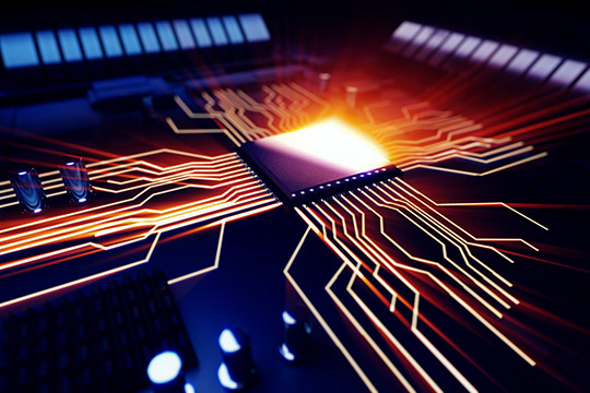
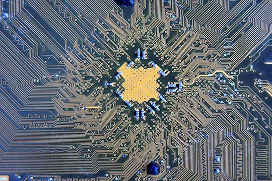
The IC design imperatives for high performance, low power consumption, and small form factors mandate increasing the number of metallization layers in IC devices. Some advanced IC chips today have more than 11 metallization levels that are fabricated in over 300 sequenced processing steps. At the heart of these processing steps lies semiconductor lithography (of which optical lithography is the most dominant form), for it determines and sets the design rule for each technology node. Each layer is defined by a geometric pattern representing circuit design information that must be transferred to the wafer surface to realize the integrated circuit. Semiconductor lithography is the process that transfers to the wafer surface the mask information for each layer of the IC. The optical lithographic exposure wavelengths span the range from 436 nm, 405 nm, 365 nm, 248 nm, 193 nm, to 13.5 nm (EUV). EUV lithography is the most advanced lithographic technology and is in production today at the 3 nm technology node in leading edge Fabs.
COURSE CONTENT
The course is divided into two main sections: fundamentals of optical lithography and advanced topics in optical lithography. The fundamentals of optical lithography section is divided into six modules, including optical lithography and its role in IC manufacturing, optical lithographic image formation, optical lithographic resist materials chemistry, practical optical lithographic resist processing, reflectivity and control, and lift-off resist pattern transfer. The advanced topics of optical lithography section is in two modules and covers materials on aberrations, low-k1 lithography, polarization and high numerical aperture effects, as well as EUV lithography. On a practical level, the course will cover exposure systems, operational principles and theories that underpin the various optical lithographic technologies; strategies, processes, and materials used in their operations; their unique features, strengths, and limitations; and specific applications to which they are targeted. Additionally, status, technical challenges, scaling, and future trends of optical lithographic technologies in general will be covered.
WHO SHOULD ATTEND
This course is intended for scientists, engineers, and technicians who wish to expand their knowledge of optical lithography.
DAY 1 – Fundamentals of optical lithography
Module 1 Optical lithography and its role in integrated circuit device manufacturing
- Principles of optical projection lithography
- Elements of optical lithography – exposure tools and systems (design considerations & properties), masks, resists
- Optical lithography in IC device manufacture
- Optical lithography roadmap and state-of-the-art today
Module 2 – Optical lithographic image formation
- Definitions – resolution, depth of focus, numerical aperture (NA)
- Diffraction & Huygen’s principle
- Image formation in a projection system
- The aerial image & its quality metrics
DAY 2 – Fundamentals of optical lithography, cont’d.
Module 3. Optical lithographic resist materials chemistry
- Overview
- Image recording in optical resist film
- Optical lithographic imaging mechanisms
- Resist materials platforms
Module 4. Practical optical lithographic resist processing
- Process flow
- Lithographic process control – contrast curves, focus-exposure matrix, Bossung plots
- Planarization
- Advanced resist processing
- Select applications of optical lithographic resists
Module 5. Reflectivity and control
- Overview
- CD control over topography
- Reflectivity control
- Top surface imaging
Module 6. Lift-off Resist Pattern Transfer
- Overview of lift-off pattern transfer process
- Lift-off pattern transfer versus other pattern transfer approaches
- Positive resist lift-off process
- Negative resist lift-off process
DAY 3 – Advanced topics in optical lithography
Module 7 – Aberrations, low-k1 lithography, polarization & high-NA effects
- Optical aberrations & their effects on lithographic imaging
- Low-k1 lithography
- Optical proximity effects (OPE) & optical proximity correction (OPC)
- Off axis illumination (OAI)
- Patterning issues & their resolutions
DAY 4 – Advanced topics in optical lithography, cont’d.
Module 8 – EUV lithography
- Overview
- EUVL exposure system
- EUVL sources
- EUVL masks
- EUV resist materials and processing
- EUVL patterning performance & challenges
- EUV scaling and extendibility