
TECHNOLOGY FOCUS
High-speed designs continue to undergo major technology changes.
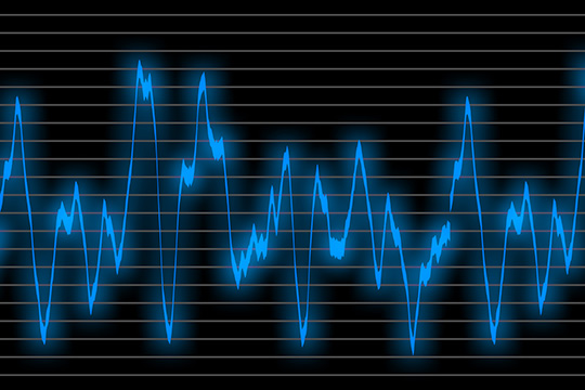
In recent years, parallel memory signalling rates are above 1000 Mbps and main-stream serial signalling is in the 5-10 Gbps range; signal rise and fall times shrink to way below 10 ps.
As a result, laminate and copper characteristics, glass-weave and surface roughness, frequency-dependent trace and component parameters, inter-symbol interference (ISI), jitter and finite bit-error-rate (BER) all need to be understood and taken into account during the design process. With the increasing utilization of transmit and receive equalizations, validation even with eye diagrams measured at package pins may not be sufficient in itself.
Today, equally challenging is the proper design of power distribution. A multitude of supply voltages and signalling levels come with reduced timing and noise margins. The allowed noise on signals and on supply rails decreases and the increasing density and bandwidth of interconnects eventually link the previously independent power-integrity, signal-integrity and EMC design domains.
COURSE CONTENT
This course uses a series of dedicated hardware (HW) and software (SW) illustrations and design examples to show and explain the underlying physical phenomena and major design rules of proper signal-integrity design.
The course gives guidance to properly select medium- and low-loss laminates, stackup and layout to ensure good signal integrity without expensive over-design.
The class focuses on signal integrity in board and system interconnects with the necessary brief overview of EMC design principles. Detailed power-integrity design and validation is covered in the companion course #56; Power Integrity: Advanced Design and Characterization. The HW and SW illustrations are shown live during the class.
The teaching methodology is based on showing and explaining good and bad design choices, discussing pros and cons of options and focusing on manufacturability and robust performance.
The course is taught with minimal mathematics, relying on the physical phenomena and a few easy-to-remember basic rules. For high-speed signal transmission, emphasis is put on the dispersive and lossy nature of cables, PCB and package traces, glass-weave, copper roughness, showing the link between rise-time degradation, jitter, eye closure and the frequency-domain scattering and transfer parameters. For power distribution and EMC, emphasis is put on the proper impedance profile of the bypass network and how to estimate and compare the worst-case transient noise of various design methodologies.
Case studies and simple exercises make the learning experience complete.
Participants will receive several of the tools and simulation files shown in the class.
WHO SHOULD ATTEND
The course is aimed at engineers, scientists and managers facing signal integrity integrity challenges in electronics designs for the computer, communications, consumer, medical, defense or automotive industries.
Only basic understanding of electronic circuits is assumed because the course is delivered through practical illustrations and examples and emphasizes the understanding of the underlying physics.
Whether you are already knowledgeable in circuit design or in the theory of signal integrity, you will find many useful tidbits and a solid explanation of the signal-integrity discipline.
Day 1
Single and Multiple Unloaded Interconnects
- Signal Spectrum, Time and Frequency-domain Solutions
- Characteristic Impedance, Delay and Performance Regions of Interconnects
- Matching and Termination Solutions and Rules; Allowable Mismatch
- Time and Frequency Domain Solutions, Network Matrices, What You Need to Know About S Parameters
- PCB Construction Rules, Stackup Options and Limitations, Cost and Reliability Considerations
Examples, live HW and SW demos: Calculation of Interconnect Parameters, Reflection, Matching, Signal Bandwidth and Spectra
Day 2
Differential, Multi-Line Interconnects
- Crosstalk in the Time and Frequency Domain, Stackup and Laminate Dependance
- Crosstalk reduction, Shield Traces, Shield Resonance
- Differential Interconnects, Effects of Imbalance, Routing Skew, Mixed-mode S Parameters, Mode Conversion, Glass-weave Effects
- Design for Multi-line Crosstalk, Simultaneous Switching Noise
- Multi-drop and Point-to-point Interconnect Characteristics, Loaded-line Periodical Filtering
Examples, live HW and SW demos: Effect of Capacitive Loading on Transmission Bandwidth, Designing for a Specific Crosstalk Goal
Day 3
Lossy and Dispersive Interconnects
- Parasitics of RLC Components, Integrated Passives
- Skin Loss, Dielectric Loss, Surface Roughness, Laminate Choice and Selection - How low-loss laminates can hurt us
- Discontinuities, Through Holes and Vias, Bends, Stubs, Design Limits
- Via Construction and Characteristics, Pad, Antipad, Drill-Size Selection
- Grounding, Shielding and EMI Rules, Dangers of Poor Cable Shielding
Examples, live HW and SW demos: Calculating Losses, How to Read S Parameters and Interpret the Impulse Response
Day 4
System Design
- Clock Sources and Drivers, Clock PLLs, Spread-spectrum Clock
- Clock Distribution, Skew, Jitter, Layout and Power-supply Rules to Minimize Jitter
- Jitter Tolerance and Jitter Transfer
- ISI, Eye Diagram, Peak Distortion Analysis, Linear Network Solutions
- Cascading High-speed Interconnect Building Blocks, S Parameters and Transfer Matrices
- Component Placement, Stackup and Layout Optimization
Examples, live HW and SW demos: Termination and Resonances in Clock Networks, Transmit and Receive Equalization, Eye Diagrams
Day 5
Simulation, Measurement, Validation
- Simulating and Modelling Vias, Planes, Bypass Capacitors
- Rules for Creating and Validating Simulation Models
- Rules to Select Simulation Tools, Settings and Setups
- Signal-integrity Simulation Pros and Cons, Simulating with S Paramenters
- Selecting Probes, Cables and Instruments for Signal-integrity Measurements
- Characterization and Validation of High-speed Systems
Examples, live HW and SW demos: Anatomy of Simulation Accuracy, Probes, Cables and Instrumentation Options
Said about the course from previous participants:
"Practical examples and experiments."
"The important trends/basics/criteria for designs."
"Real-world applications (as opposed to math)."
"The illustrations using hardware were great at bringing the theory together."
"The course has a broad approach to the subject."