
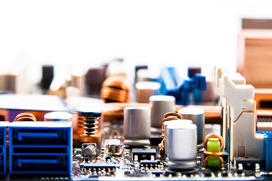
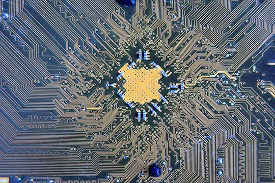
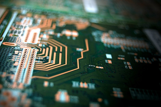
TECHNOLOGY FOCUS
The rapid growth of the microelectronics industry has historically focused on semiconductor technology, with packaging being a secondary consideration. However, with the challenges of device fabrication at advance nodes and the need for integrating diverse devices, such as sensors, MEMS, and compound semiconductors, packaging has become a primary focus for new product development. This course will provide basic information on packaging technology and provide guidance on how to choose the best packaging options in order to meet system performance and cost requirements.
COURSE CONTENT
This course covers design considerations, packaging materials, assembly processes, yield, and reliability.
WHO SHOULD ATTEND
The course is addressed to a broad audience and is not intended as a research review, although it will be taught at a high level and in many areas will require familiarity with the subject matter.
Day 1
1. Introduction;
a. Basic package requirements.
i. Cost, Size, Thermal, System Performance, Yield, Reliability
b. Basic assembly flow
i. Wire bond
ii. Flip-chip
c. Device types
i. microprocessors
ii. memory
iii. power semiconductors.
iv. sensors/MEMS
d. Wafer fabrication
i. process flow
ii. bond pads
iii. die seal
2. First level packaging
a. Wafer thinning
b. Wafer saw
i. Si
ii. SiC, GaAs, GaN
c. Substrate,
i. Lead Frame
ii. Organic
iii. Flexible
iv. Laminate
v. Ceramic
d. Die attach
i. Epoxy adhesives
ii. Eutectic solders
iii. Underfill
e. Interconnect
i. Wire bond; Au, Cu, Al, wedge bond
ii. Tape-automated bonding (TAB)
iii. Solder bumps
iv. Cu pillars
f. Mold compound
Day 2
3. Advanced Packaging.
a. Quad Flat Packs (QFP)
b. Quad flat No lead (QFN)
c. Ball Grid Array (BGA)
d. Wafer-level packaging (WLP)
i. Fan-in
ii. Fan-out (FO-WLP)
iii. Redistribution Layers (RDLs)
e. System in Package (SiP)
f. Multi chip modules (MCMs)
g. Stacked packages.
i. Package on package (PoP)
ii. Package in Package (PiP)
h. Interposers
i. 3D chip stacking
i. Wafer bonding
ii. Through-Silicon Vias (TSVs)
iii. Assembly
4. Specialized packages
a. RF
b. MEMS
c. Sensors
d. Photonics
d. Hermetic
Day 3
5. Second level packaging.
a. Design
b. Connections
i. Pins
ii. Solder
iii. Interposer
c. Component placement
d. Routing
e. Solder Masks
6. Mechanical Design
a. Vibration analysis
b. Fatigue and creep
7. Thermal Design
a. Heat transfer,
b. Thermal Resistance,
c. Thermal Interface Materials,
d. Heat spreaders and Heat sinks,
8. Reliability
a. Failure Mechanisms
i. Die Fracture
ii. Metal corrosion
iii. Wire sweep
iv. Bond pad damage
v. Wire bond / solder bump fatigue
vi. Mold compound cracking
vii. Electrostatic discharge (ESD)
viii. Electrical Overstress (EOS)
b. Reliability stresses.
i. Pre-conditioning
ii. High Temperature Storage
iii. Thermal cycle
iv. Humidity
v. Consumer vs Automotive applications
c. Accelerated Degradation Modeling
i. Reliability statistics
ii. Diffusion-related failure models
iii. Fracture-related failure models
d. Test coverage
e. Failure analysis
9. Future Trends.