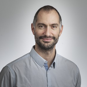
Dr. Darnon received his M. Sc. and Ph.D. from Grenoble University, France, in 2007.
Dr. Darnon then worked as a research engineer at IMEC, Leuven, Belgium, and as a research staff member in the advanced plasma group of IBM Research in the T. J. Watson Research Center in Yorktown Heights, NY, USA. His work mostly focused on plasma processes for microelectronics interconnects.
In 2009, he joined the French institute for scientific research (CNRS) as a researcher assigned to the Laboratory of Technologies of Microelectronics (LTM), where he worked on new plasma processes for microelectronics applications.
In 2015, he was assigned to CNRS/LN2 (Laboratory of Nanotechnologies and Nanosystems) at Université de Sherbrooke, Canada, where he used plasma processes to improve solar cells and integrated circuits packaging performance.
Dr. Darnon joined "Laboratoire Hubert Curien" in Saint Etienne, France in 2023 where he today works on micro-nano technologies for optics and photonic applications.
Dr. Darnon is member of the CSTIC, SPIE-AL, PESM and JNTE conference committees and has co-authored more than 100 publications, books, conference proceedings and patents. He is also an elected member of Plasma Science and Technology Division (PSTD) executive committee of the American Vacuum Society (AVS)
Editor of Microelectronics Engineering and of Micro Nano Engineering scientific journals
Dr. Darnon has been a member of the Continuing Education Institute-Europe faculty since 2011. He is the CEI-instructor on plasma etching for in-house classes at TEL, ASML, Intel, Analog Devices and others.
Course 088 Plasma Etching for CMOS Technology and ULSI Applications.
ECourse 089 Plasma Etching for Microelectronics Applications
ECourse 090 Plasma Etching for Microelectronics Applications: From Fundamental to Practical Applications


