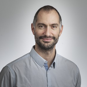
Dr. Maxime Darnon, LN2/CNRS, Sherbrooke, Canada, is teaching this Ecourse in Plasma Etching for Microelectronics Applications. From Fundamental to Practical Applications.
This is an ECourse in mixed format. Combining self-paced e-learning with live weekly sessions with the instructor. Duration in total is four weeks of effective learning. Content based on complete agenda of the public course #088. The below dates are fixed.
This course is intended to provide an understanding of plasma processes for CMOS applications and ULSI technology. You will learn the fundamental and practical aspects of front end and back end plasmaprocesses for deep submicron CMOS logic processes.
The course is based on experimental results obtained using commercial etchers connected to very powerful diagnostics of the plasma and the plasma surface interaction.
The discussions cover several aspects of etch processes of materials integrated in advanced CMOS devices,etch mechanisms, and situations that may be encountered for some important plasma processes.
Option 2: Take the short Ecourse #089 Plasma Etching for Microelectronics Applications. Combining self-paced e-learning with live weekly sessions with the instructor. Duration in total is two weeks of effective learning. Content based on the first two days of the public course #088.
Option 3: Travel and join the 4-day public live course in classroom at selected venue in Europe. View link for #088 Plasma Etching for CMOS Technology and ULSI Applications


